Category: Electronics

  • MediaTek, Cadence Partner to Accelerate 2nm Design Process

    MediaTek, Cadence Partner to Accelerate 2nm Design Process

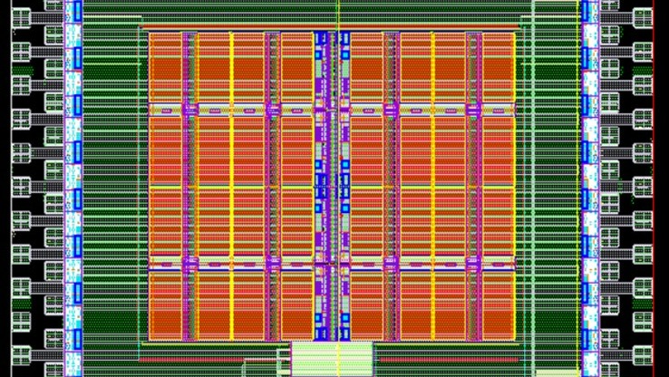
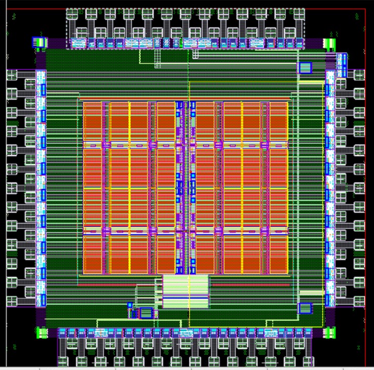
    SAN JOSE, CA, Jan 23, 2025 – Cadence has announced that MediaTek has adopted the AI-driven Cadence Virtuoso Studio and Spectre X Simulator on the NVIDIA accelerated computing platform for its 2nm development. As design size and complexity continue to escalate, advanced-node technology development has become increasingly challenging for SoC providers. To meet the aggressive performance and turnaround time (TAT) requirements for its 2nm high-speed analog IP, MediaTek is leveraging Cadence’s proven custom/analog design solutions, enhanced by AI, to achieve a 30% productivity gain.

    “As MediaTek continues to push technology boundaries for 2nm development, we need a trusted design solution with strong AI-powered tools to achieve our goals,” said Ching San Wu, corporate vice president at MediaTek. “Closely collaborating with Cadence, we have adopted the Cadence Virtuoso Studio and Spectre X Simulator, which deliver the performance and accuracy necessary to achieve our tight design turnaround time requirements. Cadence’s comprehensive automation features enhance our throughput and efficiency, enabling our designers to be 30% more productive.”

    MediaTek has used the Virtuoso ADE Suite to add its AI-based optimization algorithm to streamline future product development. This has helped its designers work more efficiently on circuit designs. Cadence’s Spectre X running on NVIDIA H100 GPUs delivers the same accuracy as Spectre X running on CPUs while delivering up to a 6X performance improvement for post-layout simulations of large, advanced-node designs.

    “Improved performance and efficiency are key to advancing today’s complex chip design processes,” said Dion Harris, director of accelerated computing at NVIDIA. “With Cadence’s Spectre X running on NVIDIA Hopper GPUs, companies like MediaTek can accelerate the verification of their complex post-layout designs, maximize analog circuit simulation performance and reduce time to market.”

    MediaTek’s analog layout team now uses the Virtuoso Layout Suite device-level router for custom digital blocks in 2nm technology, improving layout efficiency.Additionally, MediaTek is leveraging AI and Virtuoso’s open platform to create a prototyping placement and low-power prediction process. This approach improves design productivity by 30%.

    “MediaTek’s validation of our latest Virtuoso Studio release and Spectre X Simulator on NVIDIA’s accelerated computing platform demonstrates that Cadence’s continued investment in enhancing our industry-leading custom design solutions and AI tools is a game changer for our customers’ most challenging 2nm designs,” said Vinod Kariat, corporate vice president and general manager of the Custom Products Group at Cadence. “Bringing the power of AI and GPUs to Spectre X enables MediaTek to solve its large-scale verification simulation challenges even more quickly, without sacrificing accuracy.”

    Source: Cadence

  • Keysight Launches Chiplet PHY Designer 2025 for AI, Data Center Apps

    Keysight Launches Chiplet PHY Designer 2025 for AI, Data Center Apps

    SANTA ROSA, CA, Jan 23, 2025 – Keysight Technologies has announced the launch of Chiplet PHY Designer 2025, its latest solution for high-speed digital chiplet design tailored to AI and data center applications. The enhanced software introduces simulation capabilities for the Universal Chiplet Interconnect Express (UCIe) 2.0 standard and adds support for the Open Computer Project Bunch of Wires (BoW) standard. As an advanced, system-level chiplet design and die-to-die (D2D) design solution, Chiplet PHY Designer enables pre-silicon level validation, streamlining the path to tapeout.

    As AI and data center chips grow more complex, ensuring reliable communication between chiplets becomes crucial for performance. The industry is addressing this challenge through open, emerging standards like UCIe and BoW that define the interconnects between chiplets within an advanced 2.5D/3D package. When designers use these standards and ensure chiplets meet compliance, they help expand chiplet interoperability while lowering development costs and risks in semiconductor development.

    Key Benefits of the Chiplet PHY Designer 2025:

    • Ensures Interoperability: Verifies designs meet UCIe 2.0 and BoW standards, enabling seamless integration across advanced packaging ecosystems.
    • Accelerates Time-to-Market: Automates simulation and compliance testing setup, such as Voltage Transfer Function (VTF), simplifying chiplet design workflows.
    • Improves Design Accuracy: Provides insight into signal integrity, bit error rate (BER), and crosstalk analysis, reducing risks of costly silicon re-spins.
    • Optimizes Clocking Designs: Supports advanced clocking scheme analysis, such as quarter-rate data rate (QDR), for precise synchronization in high-speed interconnects.

    Hee-Soo Lee, high-speed digital segment lead, Keysight EDA, said: “Keysight EDA launched Chiplet PHY Designer one year ago as the industry’s first pre-silicon validation tool to provide in-depth modeling and simulation capabilities; this enabled chiplet designers to rapidly and accurately verify that their designs meet specifications before tapeout. The latest release keeps pace with evolving standards like UCIe 2.0 and BoW while delivering new features, such as the QDR clocking scheme and systematic crosstalk analysis for single-ended buses. Engineers using Chiplet PHY Designer save time and avoid costly rework, ensuring their designs meet performance requirements before manufacturing. Early adopters, like Alphawave Semi, attest that Chiplet PHY Designer ensures seamless operation and interoperability for 2.5D/3D solutions available to their chiplet customers.”

    Source: Keysight

  • Numem Presents MRAM-Based Chiplets to Boost AI Memory Performance

    Numem Presents MRAM-Based Chiplets to Boost AI Memory Performance

    SUNNYVALE, CA, Jan 23, 2025 – Numem is present at the Chiplet Summit to showcase its high-performance solutions in chiplet architectures. By accelerating data delivery via new memory subsystem designs, Numem solutions are re-architecting the hierarchy of AI memory tiers to eliminate the bottlenecks that negatively impact power and performance.

    The increasing demand for AI workloads and processors, including GPUs, is exacerbating the memory bottleneck. This issue arises because SRAM and DRAM are improving at a slower pace in terms of performance and scalability, limiting system performance. To address this, memory solutions with higher bandwidth and power efficiency are required, along with a reevaluation of traditional memory designs.

    Numem is transforming traditional memory paradigms with its advanced SoC Compute-in-Memory solutions. Built on its patented NuRAM (MRAM-based) and SmartMem technologies, the innovations tackle critical memory challenges head-on. The result is a groundbreaking approach to scalable memory performance, built to meet HPC and AI application needs.

    “Numem is fundamentally transforming memory technology for the AI era by delivering unparalleled performance, ultra-low power, and non-volatility,” said Max Simmons, CEO of Numem. “Our solutions make MRAM highly deployable and help address the memory bottleneck at a fraction of the power of SRAM and DRAM. Our approach facilitates and accelerates the deployment of AI from the data center to the edge, opening up new possibilities without displacing other memory architectures.”

    MRAM-Based Chiplet Solution

    At the Summit, Numem is showcasing innovative chiplets – nonvolatile, high-speed, ultra-low power solutions that leverage MRAM to overcome memory challenges in chiplet architectures. Sampling is expected to begin in late Q4’25.

    Key features and benefits include:

    • Unparalleled Bandwidth: Delivers up to 4TB/sper 8-die memory stack, exceeding existing AI memoryHBM solutions.
    • High Capacity: Supports 4GB per stack package, enabling scalability for demanding AI workloads.
    • Nonvolatile with SRAM-Like Performance: Combines ultra-low read/write latency with persistent data retention, offering reliability and efficiency. Provides the scalability and power needed to address the demands of future AI and data-centric workloads.
    • Power Smart: Game-changing power efficiency and AI Edge and Data Center based solutions with the ability to implement multi-state flex power functions (active/standby/deep sleep).
    • Broad Application Compatibility: Optimized for AI applications across OEMs, hyperscalers, and AI accelerator developers to drive the adoption of chiplet-based designs in high-growth markets. Designed with standard industry interfaces such as UCIe to facilitate ecosystem compatibility.
    • Advanced Integration: Complement other chiplet components (e.g., CPUs, GPUs, and accelerators).
    • In-Compute Intelligence: Improves memory performance by handling data flow, optimizing read/write speeds, adjusting power settings, and enabling self-testing features.
    • Proven Technology: Advanced memory subsystem IP based on proven foundry MRAM process. Offers radiation performance that mitigates exposure to soft errors.

    Numem is also demonstrating its patented NuRAM/SmartMem technology, that achieves significantly faster speeds, lower latency and dynamic power consumption compared to other MRAM solutions. It reduces standby power by up to 100x compared to SRAM, with similar bandwidth, and delivers up to 4x faster performance than HBM while operating at ultra-low power.

    Demonstrations will be given in Numem’s booth #322 on the show floor of the Santa Clara Convention Center from Jan 21-23, 2025.

  • Festo Introduces VTUX Valve Terminal

    Festo Introduces VTUX Valve Terminal

    ISLANDIA, NY, Jan 21, 2025 – Festo introduces its new valve terminal, the VTUX. The VTUX can serve as I/O, remote I/O, and decentralized I/O. These durable IP65/67-rated terminals can be placed anywhere on a machine to boost performance and speed up OEM installation. VTUX modularity results in less inventory and lower overhead costs. The VTUX is set to replace Festo’s legacy terminals.

    The VTUX valve terminal

    VTUX is both compact and lightweight, an advantage for end-of-arm tooling and conserving space on a machine or in a control cabinet. The terminal is built from a tough polymer, allowing use in welding environments.

    The key to the VTUX’s flexibility is its modular design. For high flow rates up to 670 l/min, a high flow subbase is used and for space saving needs, the compact subbase. A single valve model can be used for both subbases, which simplifies ordering, stocking, and support. High flow and compact subbases of one or four valve positions can be mixed and matched on a terminal. VTUX terminals can have up to 128 valves with up to 128 solenoid coils. The VTUX also features vacuum capability.

    The electronics side of the terminal offers the same flexibility as the pneumatics side by featuring mix-and-match modules. For example, users can add multiple analog or digital I/O modules, including I/O-Link. The modular concept continues through to the method of communication between controller and terminal. The choices include the new Festo Automation Platform (AP) for backplane speed communication in all top communication protocols. All AP-based modules appear to the control engineer to be under a single IP address that simplifies commissioning and allows smaller and less expensive PLCs to be specified. Additional communication modules include IO-Link, AP-I for decentralized I/O, and multipin connector.

    VTUX terminals are assembled and tested at the Festo Regional Service Center in Mason, Ohio. They arrive ready for installation. As a key Festo product, VTUX parts are stocked worldwide to ensure quick replacements and reduce downtime. The modular design simplifies inventory, shortens training, and speeds up troubleshooting and repairs.

    Source: Festo